Performance required for ceramic substrates and packages
Ceramic substrates and packages are used for semiconductor packages and electronic modules, of which the speedy operation and high integration are advancing, and sensor modules, of which the high precision and high sensitivity is advancing.
The performance required for these applications is as follows.
- Dimensional stability and flatness
- Supports various mounting forms (wire bonding, flip chip bonding, SMT, etc.)
- The coefficient of linear expansion is close to that of silicon
- Small size with fine wiring
- Frequency characteristic
- High reliability including heat resistance and humidity resistance
Listed below are KOA's LTCC boards that satisfy the above conditions.
Applications of LTCC substrates

- Microwave and millimeter-wave substrate for high frequency module
- Interposer for semiconductor packages
- Sensor module package such as MEMS
- High reliability module for aerospace and industrial applications
Click here for the product information on LTCC substrate
Features of KLC series (LTCC substrate)
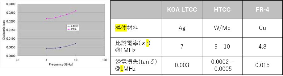
- Low dielectric loss characteristics (tan δ) and low resistance conductor with small electrical loss, which is suitable for high frequency applications
- Less variation in size and characteristics of each production lot and within each lot due to our unique manufacturing technology
- High-density wiring realized by improved stacking alignment accuracy
- Accurate control of substrate thickness and cavity shape
- Built-in resistor, inductor, and capacitor functions in the substrate and package
High frequency applications
LTCC substrates is a type of ceramic multilayer substrate. It is fired at a lower temperature than a high-temperature fired ceramic substrate (HTCC substrate) whose main component is alumina, and Ag. And it uses Ag, which has the low conductor resistance, as a inner layer conductor. Followings are the electrical characteristics it has.
- Low dielectric loss (tan δ)
- Low conductor resistance )
Low dielectric loss and low conductor resistance lead to low electrical loss at the high frequencies. Having lower dielectric loss than resin substrates, and the conductor with better electrical conduction than that of HTCC substrates, it is generally the most suitable choice for the high-frequency applications.
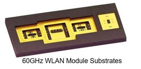
Millimeter-wave module
At high frequencies such as millimeter wave, the LTCC substrate has the advantage over the fluororesin substrate in the easiness of multilayering.
It also provides the following benefits:
- Since the coefficient of thermal expansion is close to that of silicon, the Si-based semiconductor bare chip can be mounted easily.
- High heat dissipation due to higher thermal conductivity by one digit compared with fluororesin substrate
- High moisture resistance due to its non-water-absorbing characteristic
- High-precision cavity formation enables downsizing
Above characteristics show that the LTCC substrates are suitable for semiconductor mounting, modules and packages for millimeter-wave band.
Cavity formation for packages
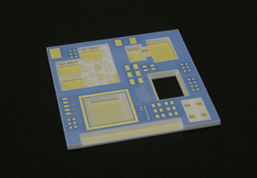
Cavity refers to the hollow space formed on a substrate, where semiconductor, sensor and other components are mounted. It enables the downsizing of module and the improvement of its characteristics.
The high dimensional accuracy of cavity and the forming of complex cavity shapes are available on KOA's LTCC. Also, the positioning accuracy of the pads for component mounting is high, making it suitable for flip-chip mounting.
It also supports complex cavity shapes for multi-chip packages.
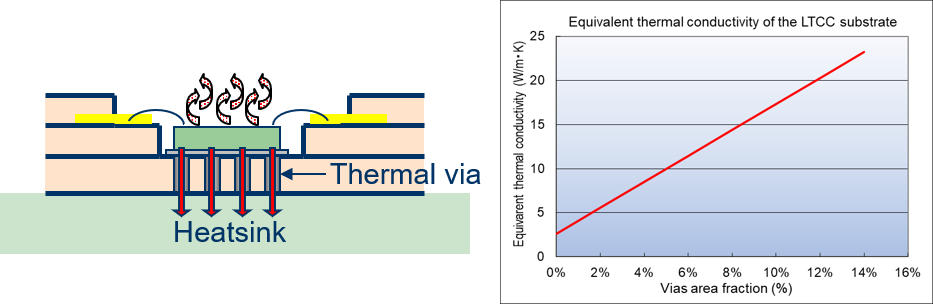
Improvement of the heat dissipation by thermal via
For semiconductor chips that generate a large amount of heat, thermal conductivity and heat dissipation can be improved by forming a thermal via directly under them.
Forming of L, C and R in the inner layer
Inductors, capacitors and resistors can be printed on the surface and inner layers. As the circuit becomes highly integrated, the environmental resistance of the module improves.
Applications requiring high reliability: No outgassing
LTCC substrate is a substrate composed entirely of inorganic components that is fired at a high temperature of 800 ºC or higher. Since it does not outgas, it is suitable for the use in environments where the outgassing is a concern, such as in vacuumed or in high temperature regions.
Supports semiconductor mounting, surface mounting, and packaging
Bare chip mounting using LTCC substrates, component mounting and BGA packaging are also available.
Click here for the details of “Custom Functional Module (Hybrid IC)”
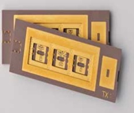
Cavity packages
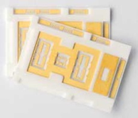
High precision cavity enables bare chip mounting and complex shapes.
Antenna modules
Three-dimensional antenna is formed by a multilayer pattern.
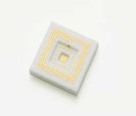
Sensor packages
Excellent heat and moisture resistance makes it suitable for the sensors exposed to severe conditions. It can be drilled and deformed and also be used in a case with a lid such as a gas sensor.
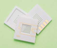
MEMS packages
Since the coefficient of thermal expansion is close to that of silicon, the thermal stress during the mounting and operation is low, making it suitable for semiconductor / MEMS chip mounting.
High frequency modules
Suitable for high frequency module substrates due to its low wiring resistance and low transmission loss.
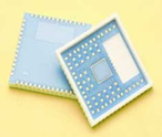
Module substrates
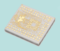
Suitable for interposers such as MCP because fine wiring can be formed.
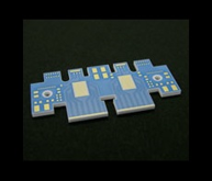
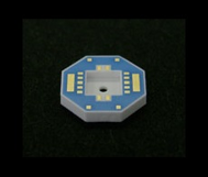
Custom shape package (example)
Complex shapes are also available.
Special shape
Button shape
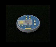
Button shape
Click here for the product information on LTCC substrate